SAW Component packaging
Abstract
Surface Acoustic Wave (SAW) filters are key components of mobile phones and TV sets. In SAW components mechanical waves propagate on the surface of a chip, so the package must provide a cavity. Solid materials on the chip would inhibit the propagation of the surface waves. Reduction of size and cost, improved reliability and electrical performance are the main trends of SAW component evolution. In the past SAW filters were exclusively soldered directly on the PCBs. Now more and more filters are integrated in modules, which are often packaged by a transfer molding process. So the ability to withstand pressures up to 100 bars was added to the list of requirements. In this paper the SAW package evolution from packages using bonded wires to flip chip packages is reviewed. Our new SAW package developments for single SAW filters, 2in1 filters and duplexers using HTCC or LTCC interposers are presented.
Introduction
Surface Acoustic Wave (SAW) filters have conquered one application after another over the past 30 years, first in TV sets and later in mobile phones [1]. Since SAW filters have a superior filter functionality and a small size, they play an important role in the evolution of mobile phones. The reduction in size of SAW filters has made a major contribution first to the miniaturisation of mobile phones and later to extending their functionality [2]. Several billion SAW filters are now produced per year, more than any other Micro-Electromechanical (MEMS) component.
In a SAW component mechanical waves propagate on the surface of a solid. To convert an electrical signal into a mechanical wave so called Interdigital Transducers (IDT) patterned on a piezoelectric solid are used. A second IDT converts this mechanical wave back into an electrical signal. Piezoelectric materials like Lithium Tantalate (LiTaO3), Lithium Niobate (LiNbO3) or Quartz are used as substrate materials. In Figure 1 the basic layout of a SAW Filter is shown.
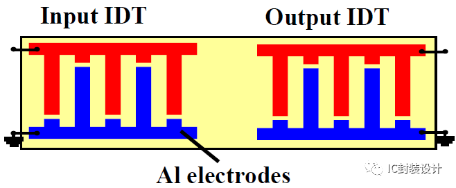
Figure 1: Basic SAW Filter Layout
The electrodes of the IDTs are arranged in a periodic pattern so only the frequencies of the electrical signal which match this pattern are converted into a mechanical wave. The velocity of the SAW wave divided by the frequency results in the SAW wavelength. The wavelength must be twice the pitch of the IDT fingers. For other frequencies the interference of the waves generated between the fingers is not constructive. This leads to the frequency filtering function. With more sophisticated layouts filters with low insertion loss within a wide frequency band and good out of band rejection near the pass band can be designed.
In mobile phones SAW components are applied in the transmit (Tx) and receive (Rx) path near the antenna. The following SAW components are used:
Single band pass filters.Input and output of the filter can be single ended or balanced.
2in1 filters which combine two band pass filters in one package. The filters can share one common chip or two chips are integrated in one package.
Duplexers which direct the transmit signals from the power amplifier to the antenna and simultaneous direct the incoming signal to the low noise amplifier. Duplexers are necessary for CDMA and W-CDMA (UMTS) telephone systems.
For the propagation of the surface wave the package must provide a cavity above the chip surface. For 2 GHz filters the IDTs are typically made of Aluminium lines with a thickness of 150nm and a width below 500 nm. These structures must be protected against humidity to prevent corrosion. This protection can be either a very thin passivation layer on the chip or a hermetic package. The resistance against corrosion is tested using high temperature at high humidity.
The package must withstand temperature changes. This is tested by temperature cycling or shock tests. For package development it has to be taken into account that the thermal expansion of LiTaO3 and LiNbO3 is anisotropic.
A cavity package is also needed for Bulk Acoustic Wave (BAW) components or Film Bulk Acoustic Resonators (FBAR). Packaging techno-logies developed for SAW filters are now also applied for BAW packaging [3].
In the past SAW components were exclusively soldered directly on the PCB of the mobile phone. Now more and more SAW filters are integrated into modules [4] [5]. A wide variety of modules are now used in mobile phones. Typical examples are:
Filter banks integrating more than two filters and impedance matching.
Frontend modules integrating filters, switching and matching mainly for GSM applications.
Transceiver modules integrating the transceiver IC, filters and matching.
PaiD modules integrating power amplifiers and duplexers.
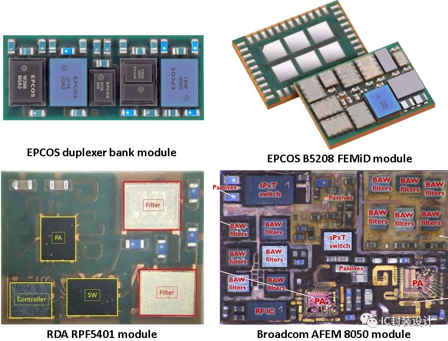
Typically modules use a LTCC or a FR4 substrate. In LTCC substrates many passive compo-nents can be integrated. On the substrate SAW filters, other passives and semiconductor ICs are assembled. The module is then closed by a metal cap, a glob top or a molding process. For molding processes pressures up to 100 bar and temperatures up to 180°C are applied. So the cavity of the SAW filter package must be robust enough to withstand up to 10 N/mm2 at 180°C. This “moldability” had to be added to the list of requirements for SAW components. This is not an easy task for miniaturized cavity packages.
Ways to integrate bare SAW chips into modules are described in [6] and [7]. As far as we know modules with bare SAW chips have not appeared on the market yet. Up to now packaged SAW components are integrated into modules.
Besides the moldability both small size and height are required when SAW components are used for modules.
The Start with Wire Bonding
First SAW components were packaged into hermetic metal packages. Bonded wires to the terminal pins connected the chip. With the introduction of Surface Mount Devices (SMD) ceramic packages with flat solder pads or lands were used. In Figure 2 such a ceramic cavity package is shown.
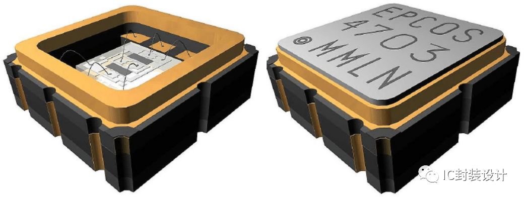
Figure 2: 3.8 x 3.8 mm2 Ceramic SAW Filter Package. Top Open, Bottom Closed.
The ceramic package is essentially a box with the SAW chip bonded into the cavity using an adhesive. Wire bonding is used to create the electrical connection between the chip and the pads inside the package. These pads are connected by vias in the ceramic or metallized castellations with the SMD pads on the bottom side of the package. The box is closed with a metal cap by seam welding or soldering.
The Move to Flip Chip Packages
It is difficult to achieve package sizes below 3 x 3 mm2 and a height below 1 mm with ceramic packages and bonded wires. So around the year 2000 the major manufacturers of SAW components switched over to flip chip packages. Besides the need to reduce the size, another reason for the move to flip chip packaging were performance limits caused by the inductivity of the bonding wires.
Most Japanese SAW component manufacturers continued to use ceramic “box” packages. They flipped the chip and used Au stud bumps instead of bonding wires [8].
At EPCOS a fundamentally new approach was applied to achieve smaller package sizes. This so called “Chip Sized SAW Package” (CSSP) will be presented in the next chapters. Since 2000 three generations of CSSP technologies have been introduced on the market. All CSSP generations use a flat cofired ceramic interposer and solder balls for the electrical connection between the SAW chip and the interposer. To achieve low costs up to several thousand components are processed simultaneously by using large ceramic panels. At the end of the packaging process the components are singulated by a dicing process. The difference between the CSSP generations is mainly the way how the cavity between chip and substrate is closed.
CSSP1
Start of production of the first CSSP generation was in the year 2000. A schematic cross section is shown in Figure 3. The area on the chip where the acoustic surface waves are activated is protected by a polymeric cavity. This cavity is made on the wafer level using the proprietary PROTEC process. A ceramic interposer made of High Temperature Cofired Ceramic (HTCC) or Low Temperature Cofired Ceramic (LTCC) is used. The electrical connection between the chip and the interposer is realised by solder balls having a diameter of 200 μm. The solder is screen printed on the ceramic substrate. In the beginning only SnPb solder was used. Later also lead free SnAgCu solder was introduced. After the soldering of the chip an underfiller is deposited between chip and interposer. The PROTEC cavity keeps the underfiller away from the active area of the chip. Copper and Nickel metal layers then seal the package hermetically.
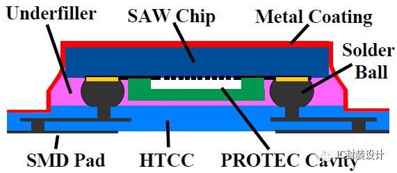
Figure 3: Schematic cross section of CSSP1
With CSSP1 technology the smallest package size is 2.0 x 2.0 mm2. As a result this technology is now being phased out for mobile phone applications.
CSSP2
To achieve a smaller package size the second CSSP generation was developed [9]. With CSSP1 technology too much space on the chip was used for the PROTEC cap and the 200μm diameter solder balls.
The production of the second CSSP generation has been running since 2002. This technology is also named CSSPlus.
In Figure 4 a schematic cross section of CSSP2 is shown. The chip is soldered on a HTCC or LTCC substrate using lead free SnAgCu solder balls. The solder balls have a diameter of 100μm. The Under Bump Metallization (UBM) on the chip side has a diameter of 125μm. Laminating a thin polymeric foil over the chips forms the cavity. A special process was developed to ensure a good adhesion of the foil and to achieve small tolerances of the foil geometry at the gap between chip and substrate. The foil is then removed at the edge of the component using a laser before the metallization of the package top. This is necessary to prevent that humidity can diffuse into the package. The top metallization is made by sputtering a plating base and plating of Cu and Ni layers. The components are separated by sawing the ceramic panel.
SAW chips have anisotropic thermal expansion. Cuts of Lithium Tantalate which are often used for mobile phone filters have a inplane thermal expansion of 8 ppm/K in x and 16 ppm/K in y direction. So the thermal expansion of a substrate with isotropic thermal expansion can never be matched to the chip. The solder bumps, the polymer foil and the top metallization of CSSP2 components are compliant so well above 500 temperature cycles are reached even for SAW duplexers where the length of the chip can be above 2 mm.
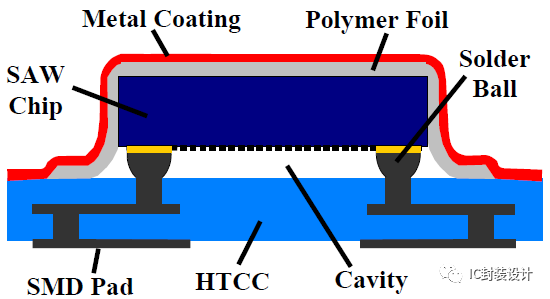
Figure 4: Schematic cross section of CSSP2
In figure 5 and 6 two examples of SAW components in CSSP2 technology are shown.
A 2in1 filter with a package size of 2.0 x 1.6 mm2 can be seen in Figure 5. 2in1 filters integrate two band pass filters in one package. Compared with two CSSP2 single filters with a package size of 2.0 x 1.4 mm2 significantly less space on the phone PCB is needed for one 2.0 x 1.6 mm2 2in1 filter.
The typical height of CSSP2 components on a 300μm HTCC substrate is 0.7 mm. With a wafer grinding process a maximum height of 0.6 mm can be achieved.
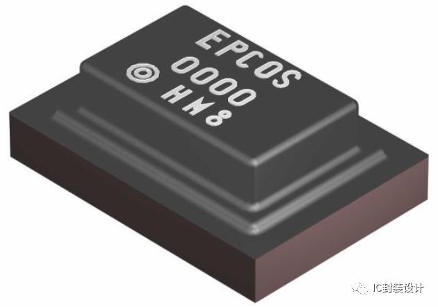
Figure 5: 2.0 x 1.6 mm2 2in1 Filter in CSSP2 Technology on HTCC Substrate
In figure 6 a 3.0 x 2.5 mm2 duplexer is shown. For a duplexer two SAW or BAW filters and a matching network are necessary. The matching network can be integrated in a LTCC substrate. At EPCOS duplexers with one SAW chip and duplexers with two BAW chips are in production. Prototypes of a duplexer combining a BAW and a SAW chip for W-CDMA Band II were completed in February 2007 [10]. In addition to the CSSP2 process an adhesive foil is placed on top of the two chips. This foil is necessary if standard nozzles are used for the pick and place process. Standard pick and place nozzles have a vacuum hole in the center so they can not hold components with do not have a flat surface.
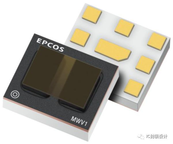
Figure 6: 3.0 x 2.5 mm2 Duplexer in CSSP2 Technology on LTCC Substrate with one SAW and one BAW chip
CSSP3 non Hermetic
The third CSSP Generation started with a non-hermetic package. In figure 7 a schematic cross section is shown. As for CSSP1 and CSSP2 the chip is flip chip bonded to a HTCC interposer. SnAgCu solder balls are used for the electrical connection between chip and substrate. Compared to CSSP2 the diameter of the solder balls was reduced. The diameter of the UBM on the chip side is 90 μm.
The package is closed by a laminated polymer foil and a glob top. This material is applied without filling the cavity between chip and substrate. Humidity can diffuse trough the foil and the glob top so this package is not hermetic. To avoid corrosion of the Aluminium structures on the chip a very thin anorganic passivation layer is deposited on the chip.
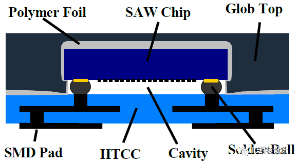
Figure 7: Schematic cross section of CSSP3 using glob top
With CSSP3 technology less space around the chip is necessary for the package. The distance between the chip edge and the component edge is only 200 μm. Due to the smaller UBM diameter a smaller chip size is possible. So a package size of 1.4 x 1.1 mm2 could be achieved for single filters. In Figure 8 a filter in CSSP3 technology is shown. By using a chip grinding process and ceramic substrates with a thickness of only 150 μm a typical height of 0.4 mm was achieved.
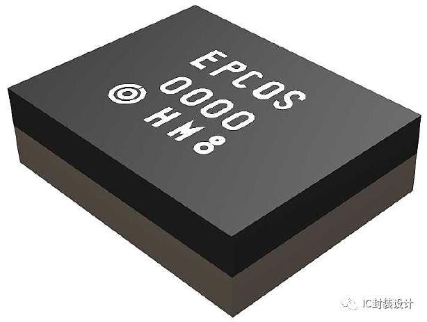
Figure 8: 1.4 x 1.1 mm2 Single Filter in CSSP3 Technology
CSSP3 Hermetic
In addition to the non-hermetic CSSP3 a hermetic third generation CSSP technology has been developed in the last two years.
For module applications thin SAW components which are stable in molding processes are required. Single and 2in1 Filters in CSSP2 and CSSP3 (non hermetic) technology are stable in molding processes up to 100 bar. For SAW duplexers which have larger chip sizes a new package development was necessary to reach stability up to 100 bars.
A schematic cross section of this package technology is shown in Figure 9. First a Copper frame and Copper pillars are patterned on the ceramic substrate. This is done by photolithography and electroplating processes.
The chip is then flip chip bonded to the substrate. After soldering the process is similar to the CSSP2 process sequence. A foil is laminated, the foil is removed on the Copper frame and a Copper/Nickel metallization is used to close the package hermetically.
The Copper frame and the Copper pillars give the necessary stability against the high pressure during a molding process. In addition, the copper frame leads to less tolerance of the foil geometry compared to CSSP2 technology. So a reduced distance from the chip edge to the component edge is possible.
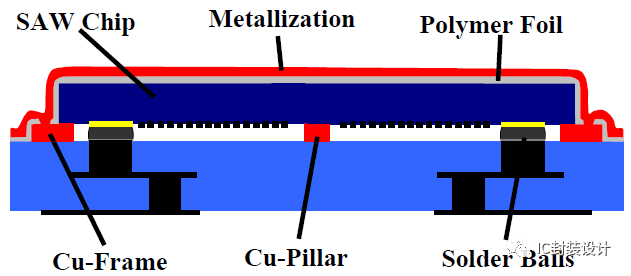
Figure 9: Schematic Cross Section of Hermetic CSSP3
Samples of duplexers with a package size of 2.5 x 2.0 mm2 and 2in1 filters with a package size of 1.7 x 1.3 mm2 have been made. Another technology for hermetic packaging of single and 2in1 SAW filters with similar size was published by Fujitsu [11] [12].
In Figure 10 a 2.5 x 2.0 mm2 duplexer in CSSP3 technology is shown. With a HTCC substrate the maximum height is 0.5 mm. With its small size and low height it is well suited for the integration into modules.
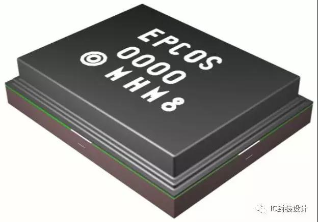
Figure 10: 2.5 x 2.0 mm2 Duplexer in CSSP3 Technology with Cu-Frame
Conclusion
Driven by the high demand of the mobile phone industry advanced cavity package technologies have been developed for SAW compo-nents. They offer low cost, high reliability and small ize. For the integration into modules moldability was also achieved.
Note:
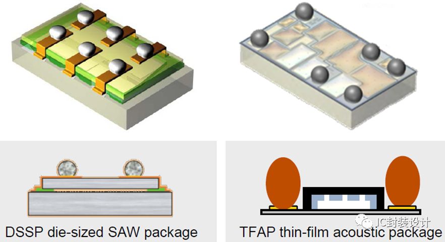
This article is published ten years ago. Today, the latest SAW packaging technology as shown below:
References
[1] C. Ruppel, L. Reindl, R. Weigel, "SAW Devices and their Wireless Communications Applications", IEEE microwave magazine, June 2002, pp 65-71
[2] P. Selmeier, R. Grünwald, A. Przadka, H. Krüger, G. Feiertag and C. Ruppel, "Recent Advances in SAW Packaging", Proc. 2001 IEEE Ultrasonic Symp., pp 283-291
[3] S. Marksteiner, M. Handtmann, H.-J. Timme, R. Aigner, R. Welzer, J. Portmann, U. Bauernschmitt, "A Miniature BAW Duplexer using Flip-Chip on LTCC", Proc. 2003 IEEE Ultrasonic Symp.
[4] P. Hagn, A. Przadka, A. Leidl, S. Seitz, C. Ruppel, "Acoustic Frontend Modules", Frequenz 59 (2005) 1-2, pp 18-23
[5] U. Bauernschmitt, C. Block, P. Hagn, G. Kovacs, E. Leitschak, A. Przadka, C. Ruppel, "RF Front-Ends For Multi-Mode, Multi-Band Cellular Phones", Third International Symposium on Acoustic Wave Devices, Ciba, 2007
[6] M. Ha, J. Lee, Y. Kwon, "Chip Scale Package for SAW Filter on the Oxidized Porous Silicon using Flip-chip Bonding and Cu plated Metal Wall", Proc. IEEE Electr. Components and Technology Conference 2002, pp 372-377
[7] V. Georgel, F. Verjus, E. Grunsven, P. Poulichet, G. Lissorgues, S. Chamaly, "Integration of SAW filter on PICS substrate using polymer sealing", IEEE, 2006, P. D. Research in Microelectronics and Electronics, pp 421-424
[8] H. Yatsuda, T. Horishima, T. Eimura, T. Ooiwa, "Miniaturized SAW Filters Using a Flip-Chip Technique", IEEE Trans. on Ultrasonics Vol. 43, No. 1, January 1996, pp. 125-130
[9] G. Feiertag, H. Krüger, P. Selmeier., "Advanced Packages for Surface Acoustic Wave Components", Proc. of Micro System Technology Conference, Munich, 2003
[10] S. Marksteiner, D. Ritter, E. Schmidhammer, M. Schmiedgen, T. Metzger, "Hybrid SAW/BAW System–in-Package Integration for Mode-Converting Duplexers", Third International Symposium on Acoustic Wave Devices, Ciba, 2007
[11] O. Kawachi, K Sakinada, Y. Kaneda, S. Ono, "Packaging of SAW Devices with Small, Low Profile and Hermetic Performance", Proc. 2006 IEEE Ultrasonic Symp., Vol. 27, pp 281-282
[12] O. Ikata, Y. Kaneda, S. Ono, K. Sakinada, O. Kawachi, Y. Tanimoto, "Miniaturized SAW Package with Hermetic Performance", Third International Symposium on Acoustic Wave Devices, Ciba, 2007


